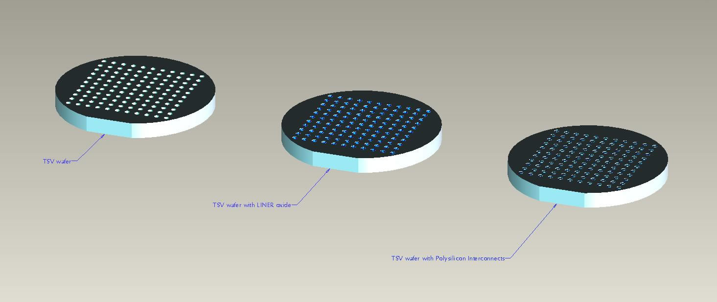
IceMOS Technology have developed an innovative and powerful through-wafer interconnect technology which can allow device designers in both standard IC and MEMS device industries overcome packaging problems associated with their designs. Using this interconnect solution allows many of our customers to migrate their designs easily to a wafer level package with solder bumped contacts.
The IceMOS Technology solution is a preprocessed substrate which is delivered to the customer with the interconnect already formed within the substrate. This substrate is fully CMOS compatible.
All interconnect is performed using through wafer etching and refill using heavily doped polysilicon. The wafers meet all standard specifications for surface metallic contamination, planarity and particle count. We have verified stable substrate performance up to diffusion temperatures of 1200C.
IceMOS customised TSV solutions are used in the following fields:
- SOI solutions for MEMS/MST
- Bio MEMS
- RF MEMS
- Smart Power
- Advanced Analog ICs
IceMOS will develop customer specific through-wafer interconnect solution in partner, taking the preferred interconnect pattern and implementing it on the wafer for easy connectivity to a circuit or sensor. The TSV may be beside or below existing bond pads. The design is optimised and fully customised to the customer’s requirements